It is used for detecting any defects in the wafers before final packaging and is ideal for scanning small sections of a die to identify specific hard to detect systematic and random defects.
E beam wafer inspection.
On the other hand the dark field inspection system can detect at high speed and is intended for the defect inspection of a large number of wafers.
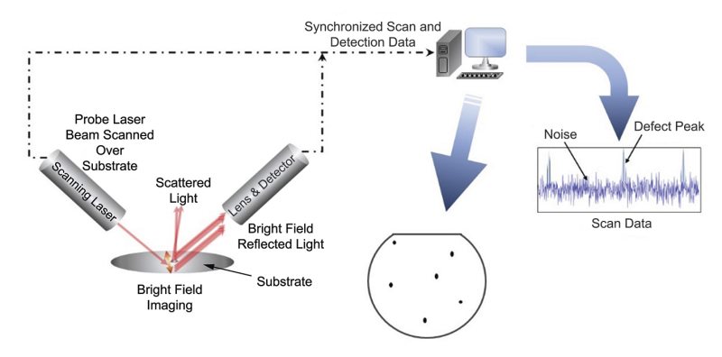
In the electron beam inspection system electron beam is irradiated onto the surface of the wafer and the emitted secondary electrons and.
E beam wafer inspection electron beam eb imaging is also used for defect inspection especially at smaller geometries where optical imaging is less effective.
At the time hmi was the world s largest supplier of e beam wafer inspection tools.
E beam inspection is being used to a limited extent in production for statistical sampling.
In general the bright field inspection system is intended for the detailed examination of pattern defects.
In 2016 asml holding entered the e beam wafer inspection market by acquiring hermes microvision hmi.
E beam wafer inspection system is a fabrication tool for semiconductors that utilizes electron beam scanning of integrated circuit ic components or wafers.
The system is used to identify wafer defects prior to the.
It identifies the defects in wafers.
In e beam inspection the stage moves the wafer to a given location.
Regardless e beam inspection is making progress on several fronts.
In r d it is indispensable said sundararajan of w r.
Eb inspection can provide material contrast with a dynamic range of resolution much larger than optical inspection systems.
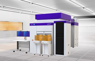
The esl10 e beam patterned wafer defect inspection system captures and identifies defects not found by other inspectors reducing the cycle time required for solving critical yield or reliability issues.
Milpitas calif july 20 2020 prnewswire today kla corporation nasdaq.
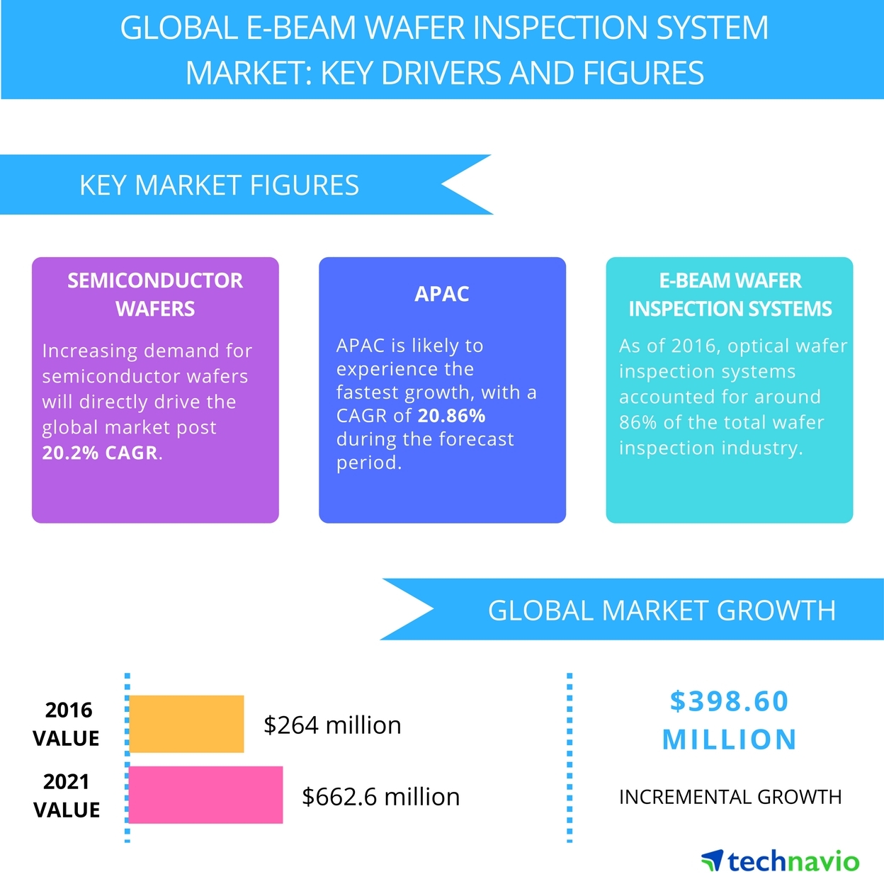
E beam wafer inspection system market will exhibit an impressive 17 5 cagr between 2017 and 2025.
The e beam scans a select part of the wafer and the image is collected.
Recently asml hmi introduced their first jointly developed system.
E beam wafer inspection system refers to a semiconductor fabrication tool based on electron beam scanning of integrated circuit ic components or wafers.
E beam wafer inspection system industry is projected to reach us 1 06 bn by the end of 2025 from a valuation of us 248 3 million in 2016.